China Solder Paste: Using Multi-Level Stencils for Soldering SMT Components
The need for soldering SMT components with varying china solder paste heights is more than it was ever before. The world is rapidly transitioning towards smaller electronic devices. And while this change has made the lives of consumers easier. It has presented unique challenges to circuit board manufacturers.
China solder paste is the binding component in SMT soldering. The parameters of solder printing define the success of a PCB printing job. But with each innovation, executing a screen printing job with perfection is becoming increasingly difficult. Especially when it comes to soldering different-sized components.
In this article, we will discuss some challenges that SMT soldering faces in face of modern technologies. Then we will discuss how electronic solders are overcoming challenges in the way of soldering SMT components with varying solder paste heights.
SMT Soldering with China Solder Paste: An Introduction
The size of electronic devices has decreased while their operational power has increased. Now a powerful electronic device is so small and lightweight that it can easily sit on top of our wrist. And SMT components are to give credit for this development.
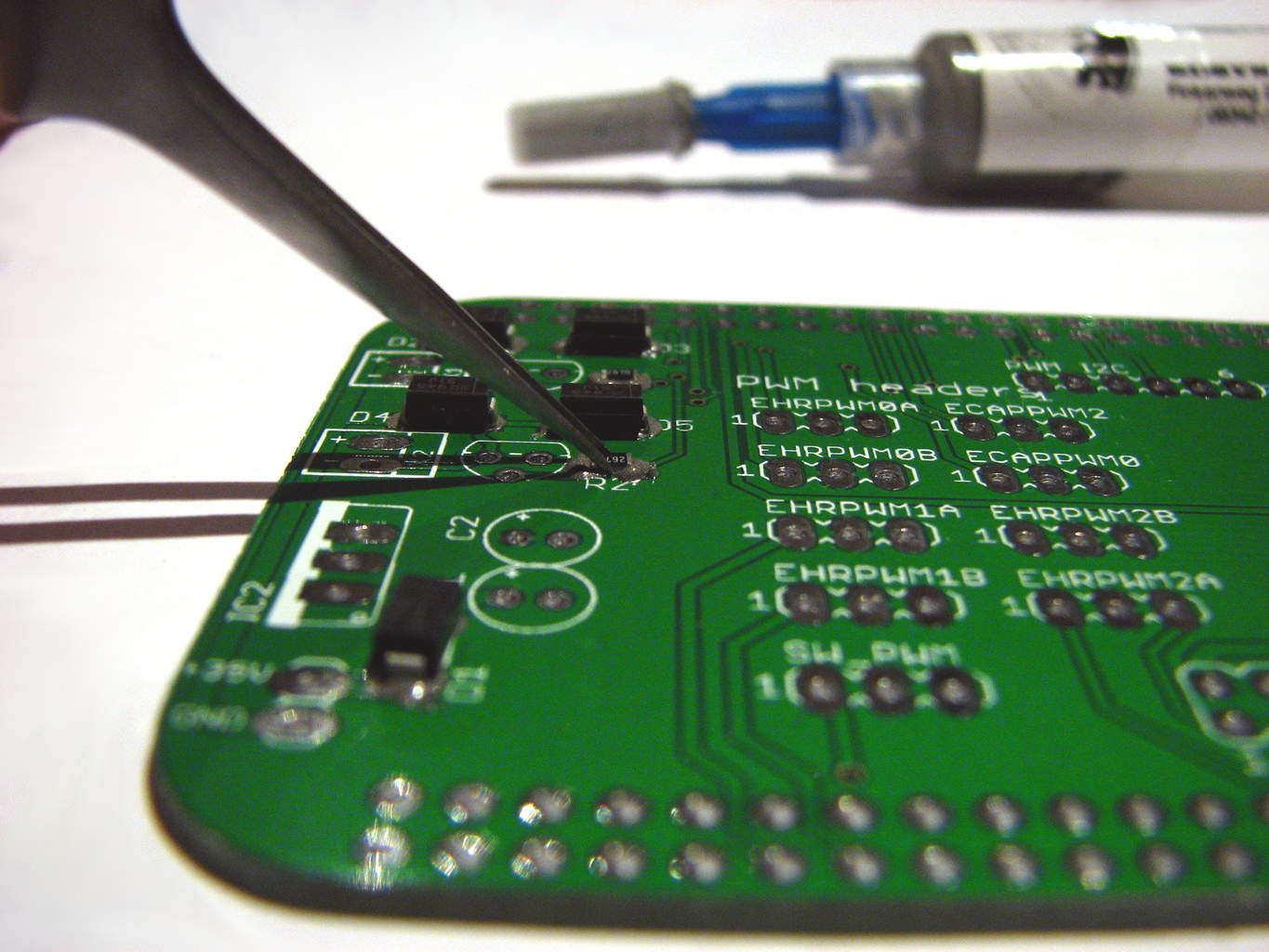
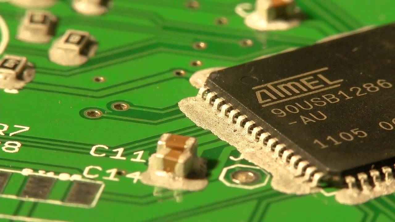
SMT components are smaller electric components that you can solder directly on the circuit board. The process of soldering SMT components directly on the PCB is what we call SMT soldering.
SMT soldering has played a vital role in the shift of electronics from large room-filling devices to small fits-in-your-palm gadgets.
Modern Technologies and the Challenges with Screen Printing
Screen printing is the process of depositing China solder paste onto a circuit board through the apertures of a stencil. It is the most important process of the entire PCB manufacturing process.
Studies suggest that around 60% of the defects that become apparent in the PCB, later on, are due to the defects in the printing process.
As crucial as the screen printing process is, electronics manufacturers, struggle with its perfect execution due to the innovations in the industry around every corner. The need for smaller components mounted on the circuit boards keeps the manufacturers on edge because then they need unique stencils to fulfill the unique requirements of the innovative product design.
Moreover, some product designs include a mixture of old and new components. That means they require circuit boards that carry smaller and large SMT components soldered side-by-side. This means the solderers cannot use one stencil to print an entire circuit board in one go.
China Solder Paste: Importance of Varying Height
Optimizing the height and thickness of china solder paste in SMT soldering is crucial. It ensures the reliability of the solder joint and minimizes the risk of defects further down the line.
If the thickness of china solder paste is more than the size of the components, it could lead to defects such as bridging and lack of joint formation.
Additionally, too little china solder paste can lead to the formation of voids in the solder joint which will reduce the joint’s electrical conductivity.
Previously, PCBs carried same-sized components, and manufacturers used one stencil for printing an entire circuit board. However, with the latest PCBs requiring a variety of component sizes, manufacturers can no longer use one stencil for screen printing one PCB.
To accommodate the needs of electrical manufacturers, solder paste stencil manufacturers are continuously optimizing stencil sizes. Over the past few years, the stencil thickness has reduced from 0.008 inches to 0.004 inches. However, this is still not enough for soldering different-sized components.
Two Ways to Solder SMT Components with Varying China Solder Paste Height
If you are looking for soldering SMT components with different china solder paste heights on a single PCB, you will come across two options. These are: solder dispensing or using multi-level stencils.
Solder Dispensing
Solder dispensing is a viable option for hobbyists or for people who make only a few PCBs at a time. In solder dispensing, you can use a solder dispensing unit to inject the required thickness of china solder paste on the circuit board.
Printing circuit boards with solder dispensing is a long and tedious process. It is time-consuming and hence isn’t viable for manufacturers who produce circuit boards in bulk.
Using Multi-level Stencils
Multi-level stencils are the preferred choice of PCB manufacturers because they offer the same turnaround time as normal stencils while printing circuit boards with different china solder paste heights.
Multi-level stencils do not have a uniform thickness, like standard stencils. These stencils vary in their thickness to accommodate the dimensional requirements of the SMT components that are to be soldered on the PCB.
The thicker side of the stencil will deposit an increased thickness of the china solder paste. While the thinner side will deposit a smaller height. Hence, depending upon your PCB design, you can determine the dimensional layout of the stencil.
Types of Multi-level Stencils
Multi-level stencils are classified based on how they are made to vary in their thickness. There are two types of multi-level stencils including stepped-stencils and additive stencils. Both of these stencils are made by altering standard stencils.
Stepped Stencils
Step stencils have been in use for the past ten years. These stencils are made by taking a thicker stencil and removing the material on areas where there is a need for a thinner stencil.
Chemical etching is the most common method to produce step stencils. However, other processes like laser cutting and milling are also not uncommon for making step stencils.
Additive Stencils
Additive stencils are an alternate of stepped stencils. These stencils are made by adding a layer of the standard stencil to the base stencil thereby increasing its thickness.
In this way, the area that has to deposit a small thickness of china solder paste is left thinner while the area which has to deposit a larger height of the solder paste is made thicker by adding subsequent stencils.
Pros and Cons of Multi-level Stencils
Multi-level stencils have their pros and cons. Whether you will reap benefits from designing custom multi-level stencil or will suffer a loss from them depends on your PCB printing scale.
Pros:
Printing Flexibility
Custom-made multi-level stencils provide printing flexibility, unlike standard stencils that you get off the shelf. These stencils allow you to print a circuit board with varying china solder paste heights while minimizing lead time and maintaining the quality of the solder joint.
Faster Lead Time
The only alternative to multi-level stencils for printing PCBs with varying solder paste heights is a solder dispensing unit. However, as mentioned above, solder dispensing can be a tedious process and has a turnaround time twice that of multi-level stencils.
Therefore, with regards to screen printing, stencils have a major benefit in that they save time and allow for greater yields and better profits.
Cons
Tedious Design Process
While using a multi-level stencil can save you a lot of time while printing PCBs with varying china solder paste heights, designing the stencils can be tedious.
The stencil you design may not be perfect on the first go. And you’ll have to go through several iterations before you can get your hands on a stencil that fits your requirement.
Fine Pitch Components
Multi-level stencils may not be viable when printing for fine pitch components. If the component requiring a greater thickness of solder paste is closer to the stepped-down area of the stencil, then the large component solder pad will get insufficient solder paste, and this may result in a bad solder joint.
Conclusion
With the miniaturization of electronic components, the importance of SMT soldering has increased. However, some applications require you to solder small and large SMT components on the same PCB, which presents difficulty.
This challenge in SMT solder can be overcome by using multi-level stencils. These stencils are made to deposit varying heights of china solder paste onto the solder pad and ensures that each component solder pad gets optimum height and volume of the solder paste.
For More Information, Reach Out To Us Today!