What You Need To Know PCB Solder Paste
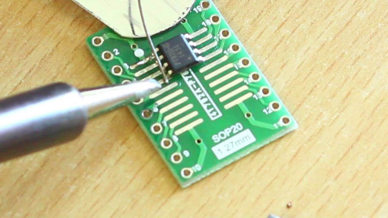
PCB solder paste printing is a common technique to attach an SMD (surface-mount-device) to PCBs (printed-circuit-boards). And, it is a fact that most assembly defects arise during the process of stencil printing. Moreover, the process of solder paste printing is solely liable for the joint development of leadless technologies, like LGA (land-grid-array) and QFN (quad-flat-no-lead) components. Therefore, it is a crucial aspect in the reliability of the devices in the long run.
This document will discuss the different effects of the solder paste volume on the PCB assembly. We will take some recent studies and experiments as a reference for value. Therefore, let’s start this meaningful discussion by discussing the solder paste printing approach and design. After that, we will discuss different effects and possible defects to avoid.
PCB Solder Paste Printing Approach and Design
Stencils with altered aperture scopes at specific locations for QFN and LGA package footprints are designed for varying volumes of solder paste pledged during the stencil process. Engineers measure the volumes of solder paste with the help of the PCB solder paste inspection program. For evaluation of the assemble yield, altered stencil designs are necessary to generate low-volume solder paste. In addition, engineers use ATC (accelerated-thermal-cycling) to check the reliability of solder joints.
Failure analysis determines whether or not the failure relates to low volumes of the solder paste locations. Several studies are available addressing solder paste printing and enhancements for the printing procedure. Apart from that, several other studies on solder joints reliability are available, utilizing thermal cycling to generate failure and access the solder joint’s reliability.
A recent Sriperumbudur thesis discusses the volume of PCB solder paste and the way it is related to the reliability of solder joints for LGA (land-grid-array, BGA (ball-grid-array), and QFN (quad-flat-no-lead) components. This paper targets to correlate the volume of solder paste to the reliability of solder joint for lead-frame components and passive-chip components. Generally, engineers create stencil files and circuit board data simultaneously.
The initial layers of the stencil are usually created simultaneously, like copper layers. Printing issues will occur if you make stencils using original figures without adjustments. Such issues may include solder balling and bridging, etc. Stencil manufacturers and engineers alter the design of stencil to improve printing and avoid printing defects.
Design Guidelines for Modifications
Usually, engineers follow Design Guidelines IPC-7525 for modifications. It is standard practice for reducing 10-50% area stencil apertures in comparison to copper pads. It reduces the printed solder paste volume significantly. You may also reduce the stencil width if you use smaller passive parts or 0603 metric (02021 Imperial) or µBGA (fine pitch micro-ball grid array. It is essential for maintaining the ratio of aperture area above 0.66 values that is an industry-standard to follow.
Reliability of PCB Solder Joints
Reducing the thickness of the stencil also decreases the printed solder paste volume. Ensure that solder joints you create using a reduced volume of PCB solder paste meet the J-STD-001 and IPC-A-610 criteria. But what about the reliability of solder joints? It is essential to know about the lowest paste volume limit needed to produce a reliable joint. It is also necessary to know whether the joints will last for a long time of the PCB assembly.
To ensure all such things, engineers have to perform reliability testing using several solder volumes to define the lowest limit of paste volume they can use. The standards J-STD-001 and IPC-610 allow them for different volumes of solder. The criteria of inspection in the said standards focus on the following things:
- Angles of solder wetting
- Coverage or spread of the solder, including de-wetting or wetting
- Exposed base metal
- Blowholes or pinholes
- Incomplete reflow or cold solder
- Bridging and excess solder
- Mid-chip beads and solder balls
- Distributed solder paste joints, shrinkage cracks, or hot tears
- Components position concerning pads
- Cracked or fractured solder
- Length, width, and height of solder joints
- The thickness of the solder
If you do not pay focus on any of the above-listed points, then the inspection criteria would be affected. The boards assembled for the above study went under inspection according to such standards. Engineers analyzed the pull and shear strength through solder joints. Engineers performed thermal cycling and accumulated extra pull and shear strength data. The data of joint strength and inspection was connected to the volume of PCB solder paste.
Findings
According to different studies, solder joints made with a small volume of paste last longer in the ATC than to the intentionally low joints volume. Transfer efficiency statistics for good reliability and good assembly proved perfect for both QFN and LGA devices. A lower limit of volume is ideal for the leadless device(s) that should not affect reliability and yield significantly in thermal cycling. All these findings are taken from the recent studies, including the ones we have mentioned above.
Value/Originality
There is no vast amount of literature available on limits of volume tolerance for the PCB solder paste concerning reliability and assembly yield. Manufacturers often utilize ±30 or ±50 percent volume of the stencil aperture without any evidence of efficiency in defining solder joint’s reliability and yield. However, we may find additional literature on this in the future from more studies and experiments.
Summary
Several studies have revealed specific guidelines on the volume of printed solder paste for specific parts regarding reliability and manufacturing yield. We can use several paste volumes for creating reliable solder joints. However, the solder joints may be unreliable if you use too low solder volume. Modifications in the volume of solder paste can encourage several defects. However, you can still correct these defects. PCB assemblers should create standards on their own for the reliable volume of solder paste according to the parts they use.
We hope this document helped you understand the effects of solder paste volumes on the PCB assembly. However, the statistics and information we shared in this document are taken from recent studies and experiments. Therefore, you must follow the essential guidelines and suggestions we have discussed in this article for reliability.
For More Information, Contact Us Today!

